

Samsung on Wednesday revealed its update roadmap for its most advanced chip nodes serving AI chips. The South Korean tech giant also introduced a new turnkey service that aims to leverage its diverse chip businesses to entice companies such as Nvidia and AMD to use its foundry or sign a contract. chip co-manufacturing, services for their AI chips.
The announcement marks a shift in focus for Samsung Foundry, the company’s contract chip manufacturing business, to chips for AI and high-performance computing (HPC) rather than mobile processors. dynamic.
Also: Samsung’s chip division wants to regain the top spot: What’s going on?
The company noted that Samsung Foundry’s AI sales grew 80% over the past year and that the company is making significant strides in diversifying its customer base and application areas amid market demand. school is increasing. It also said the tech giant aims to have more than 50% of its foundry revenue come from outside the mobile sector.
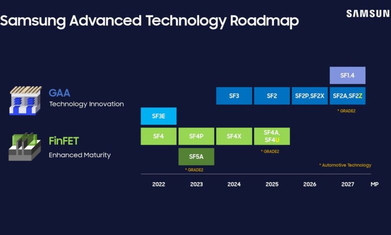
At the Samsung Foundry Forum, an annual event for the foundry industry with this year’s theme of Empowering the AI Revolution, held in San Jose, the company demonstrated its 2 nanometer (nm) process nodes and The new 4nm, called SF2Z and SF4U respectively.
The SF2Z combines what is called a back-side power distribution network (BSPDN) with a conventional 2nm node (Samsung’s SF2), where the power rails are placed on the back of the wafer. Current chips have all the on-chip components such as memory, logic, and power rails on the front of the wafer. Other contract chipmakers are also preparing their own BSPDN technology __ Intel calls it PoweVia and TSMC calls it Super PowerRail which they are also planning to apply to their 2nm or sub-node chips .
Also: Samsung establishes HVAC joint venture with Lennox to expand business in North America
According to Samsung, placing the power rails on the back will help increase power, performance and area (PPA) as well as voltage drop. SF2Z targets AI and high-performance computing (HPC) chips and will launch in 2027. Samsung had previously said that SF2 would launch in 2025 before the forum.
Samsung was the first to start production 3nm comprehensive gateway (GAA) node in 2022. At the forum, Samsung noted that its GAA process is maturing in terms of performance and yield and that a second-generation 3nm node called SF3 will launch later this year. The company said GAA will also be applied to its 2nm node next year.
Samsung is adding various variants to its 2nm node, with a particular focus on AI. Image: Samsung
Meanwhile, SF4U is a variant of the 4nm SF4 process, offering the ability to increase PPA using optical miniaturization, where the customer’s existing die design is scaled to fit the newer button. This helps them save costs because major architectural changes in chip design are not required to migrate to a more advanced node. SF4U will launch in 2025 while Samsung is already making SF4 available to customers. The South Korean tech giant also reiterated that its 1.4nm (SF1.4) node will launch in 2027 and is also preparing for sub-1.4nm chips.
Samsung also unveiled a new turnkey foundry platform called Samsung AI Solutions. The platform is provided by Samsung’s three business units in the chip division: Foundry, Memory and Advanced Package (AVP).
Also: Samsung Galaxy Ring: Features, price, availability and everything else we know
According to the company, the platform integrates the “unique strengths” of each of these business units, allowing Samsung to provide solutions to customers tailored to the specific requirements of their AI chips. Overall, Samsung says, it will provide more bandwidth in a compact design, reduce power consumption and improve signal integrity.
As the only chipmaker that can supply memory chips to go with customer chips and produce and package these chips, Samsung says this helps streamline supply chain management and reduce time to market to customers. The company said Samsung AI Solutions helps customers improve overall processing time by 20%. The Korean tech giant said Samsung AI Solution will be offered with co-packaged optics (CPO) __ where even the optics are packaged __ by 2027.
Samsung’s decision to add more variants to its process nodes makes sense as a strategy for AI, an umbrella term that actually encompasses many different types of chips designed for different tasks and tasks. different scales. Some are created for ChatGPT and other major language models. Some are for vision and image processing for use in drones and display devices. Others are AI accelerators for data centers.
According to market research firm Omdia, the global foundry market is expected to grow by an average of 18.1% per year from 2023 when it is worth $103.55 billion to 2027, when it is expected to be worth $201.28 billion. The research firm’s forecast notes that growth in advanced nodes 3nm and below will be most pronounced at an average of 92.3% per year over the period.
Samsung is the world’s largest memory chip maker and the second largest contract chip manufacturer. Its memory business is trying to win Nvidia is a customer of the HBM3E chip, used in conjunction with the GPU manufacturer’s AI accelerator.


